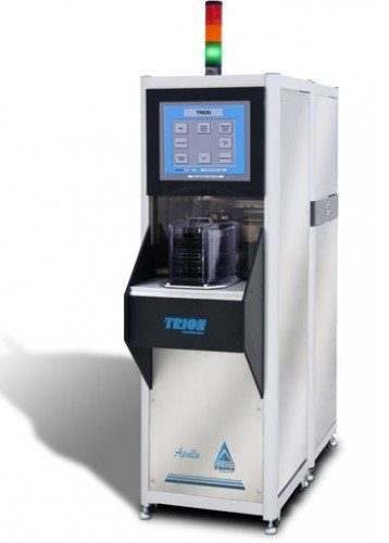
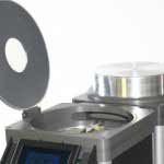
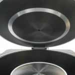
Plasma systems or vacuum deposition and etch systems are primary tools of semiconductor process or fab or research in nanotechnology. Miniature sensor development or chip development rely on Chemical Vapor deposition and Plasma Ion etching tools for device fabrication. Chemical vapor deposition and etch systems use variety of gases – some toxic some inert to develop a process for fabrication of on-wafer device chips. Parallel plate plasma chemical vapor deposition or Reactive Ion Etching tools are commonly used in developing variety of semiconductor chips. Chemical Vapor deposition systems can be a simple CVD tools having a small furnace and gas inlets with heating mechanism or it can be a plasma-based system in which plasma is used as inert atmosphere to avoid impurities in the fabrication process. Etch systems also use to avoid contamination in the process. Different configuration such as PECVD/HDPECVD , RIE/ICPRIE are available for chemical vapor deposition and etching requirements.
PTek, located at Hyderabad, is engaged in offering best equipment and services to the industry and research institutes in the field of Air Filter Testing, Aerosol generation, Semiconductor Process Equipment & Cryogenic systems.
Products
GET IN TOUCH
CONTACT INFO
H.No. 12-10-212,
Sitaphalmandi.
Secunderabad - 500 061
(Telangana)
India
9490118703
sales@thinkptek.com
www.thinkptek.com
Registered under MSME, Govt of India